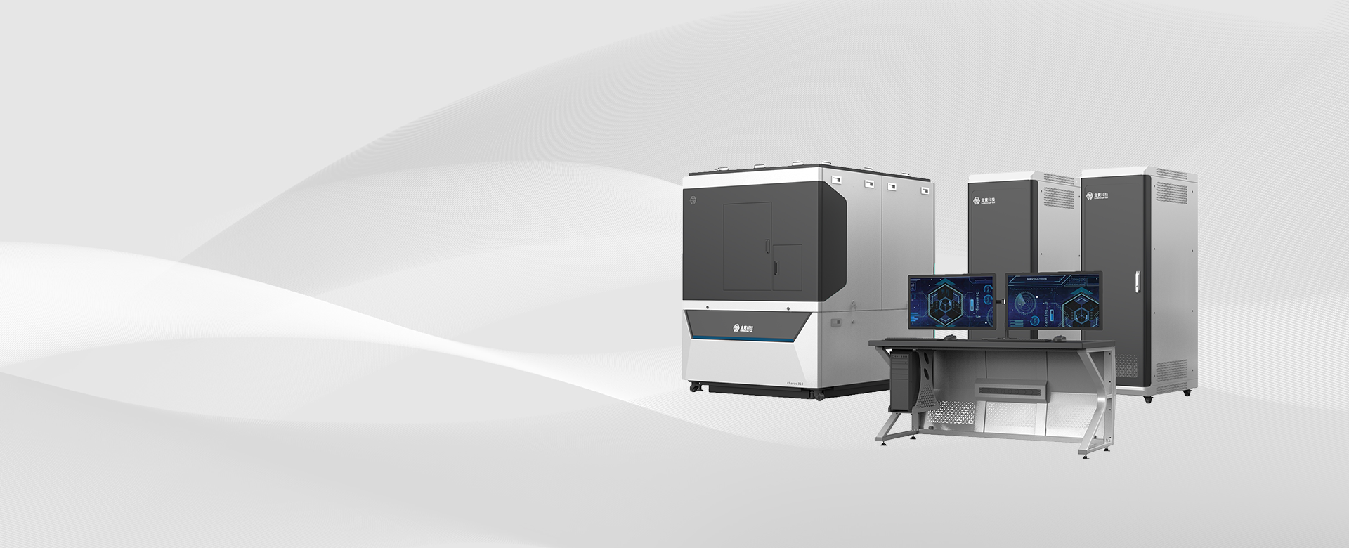


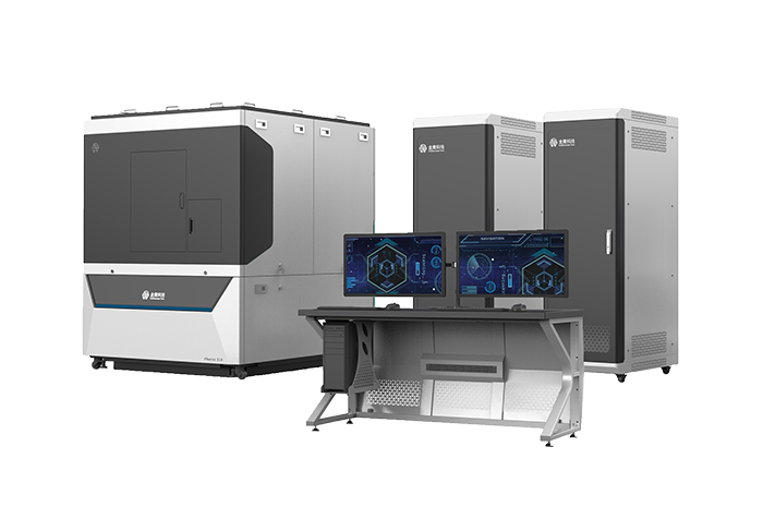
Electron Beam Lithography system——Pharos 310

Electron beam lithography refers to the process of creating patterns on photoresist using a focused electron beam, an extension of the photolithography process. The electron beam lithography system is the hardware platform that enables this technology, with system performance determining key parameters such as critical dimensions, stitching, and overlay accuracy in the exposure process.
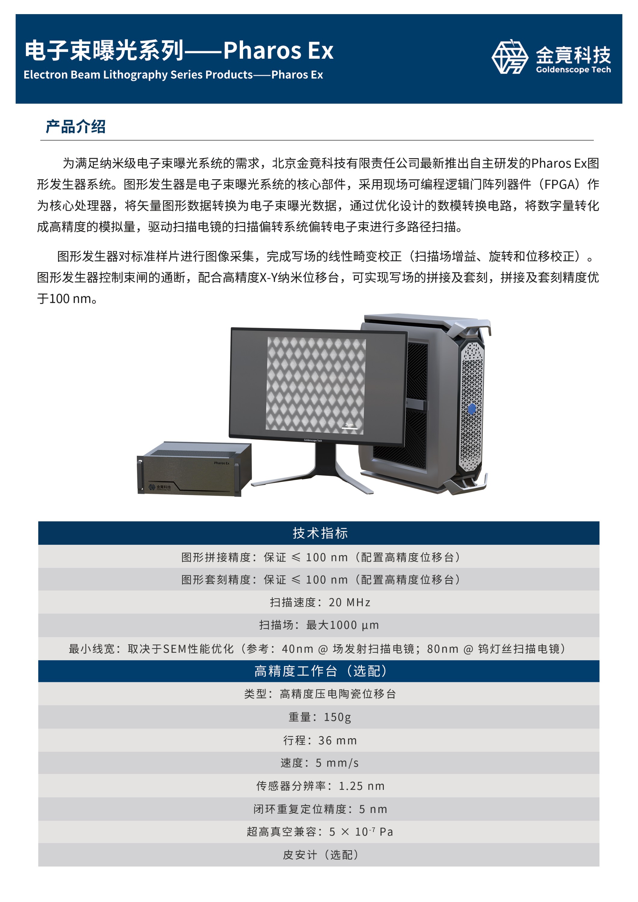
Goldenscope Technology has achieved technological breakthroughs in the core components of electron beam lithography processes and equipment, and has become the first in China to launch the independently innovative, quality-controlled, and high-performance electron beam lithography system: Pharos 310. Several key technical indicators of this system have reached international first-class standards, achieving the development goal of replacing imported electron exposure equipment with domestically produced, independently controllable alternatives.
The Pharos 310 can expose critical feature sizes of less than 15 nm on 4-inch substrates. The Pharos 310 system is a powerful tool for easily exposing complex layouts, making it an essential instrument for submicron to nanometer-scale lithography technology research and development under laboratory conditions.
Applications of Electron Beam Lithography system:
· Semiconductor Manufacturing: Used for the fabrication of integrated circuits, chips, and other semiconductor devices.
· Nanotechnology Research: Plays a crucial role in the development of nanomaterials and nanodevices.
· Optics: Used in the production of photonic crystals, optical waveguides, modulators, metasurfaces, and other optical components.
· MEMS (Micro-Electro-Mechanical System): Utilized in the fabrication of nanostructures.
· Biochips: Applied in the manufacturing of biochips.
· Materials Science: Research on the surface properties and structures of materials.
· Quantum Technology: Used in research and development in quantum computing, quantum communication, and related fields.
Electron Optics Parameters
· Electron Emission Source: Schottky emission source with a lifespan of no less than 1,500 hours.
· Acceleration voltage: 200eV-30 keV
· Electron beam current: 5pA-200nA
· Electron beam spot size: ≤ 2.0nm@30keV
· Writing Field Speed: Up to 20 MHz pixel frequency.
· Maximum Writing Field Size: 500 µm × 500 µm.
· Resolution (Minimum Line Width): ≤15 nm*.
· Stitching Accuracy: ≤ ±50 nm (mean+3sigma).
· Overlay Accuracy: ≤ ±50 nm (mean+3sigma).
· Sample Stage Movement Range: 100 mm.
· Maximum Sample Size: 4-inch wafer.
Standard Configuration
· Sample Stage Positioning: Equipped with a laser interferometer for precise positioning.
· Vacuum Readiness Time: From sample loading to achieving working vacuum conditions in the sample chamber, the process takes no more than 10 minutes.
· Automatic Loading System: The system features an automatic sample loading mechanism, requiring no manual intervention during the loading process and includes an optical navigation system.
· Control System: Operates on a Windows platform, with lifetime free upgrades as long as hardware permits.
· UPS (Uninterruptible Power Supply): One UPS unit is provided.
· Air floating vibration reduction system: Ensures the overall stability of the electron beam lithography system.
*Process Details:
· Photoresist: PMMA 950K A2.
· Photoresist Thickness: 60 nm.


Professional Systematic Training


Rich Application Experience


Timely And Efficient Response


Excellent Service Experience


GOLDENSCOPE TECH GOLDENSCOPE TECH GOLDENSCOPE TECH GOLDENSCOPE TECH GOLDENSCOPE TECH GOLDENSCOPE TECH GOLDENSCOPE TECH GOLDENSCOPE TECH GOLDENSCOPE TECH GOLDENSCOPE TECH


 Product Introduction
 Technical Specifications
 Download Center
 Service Support