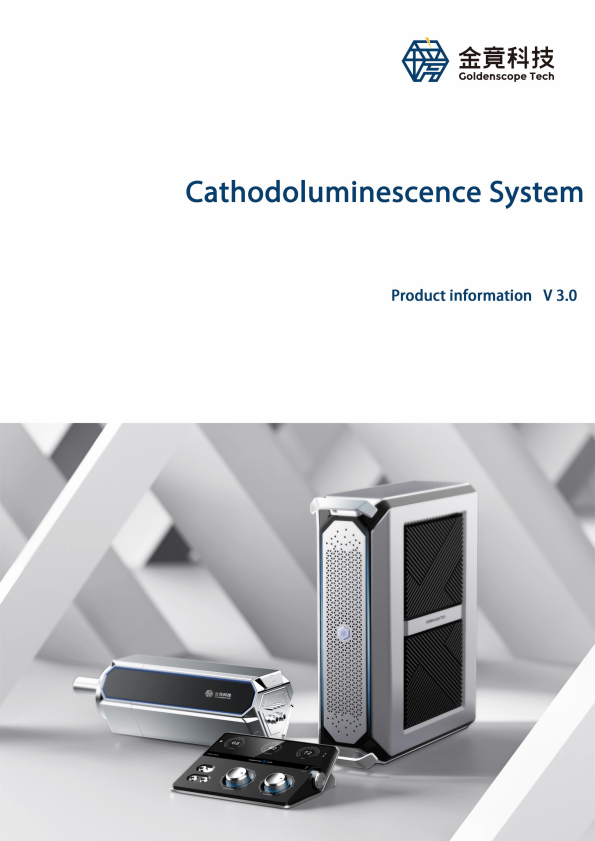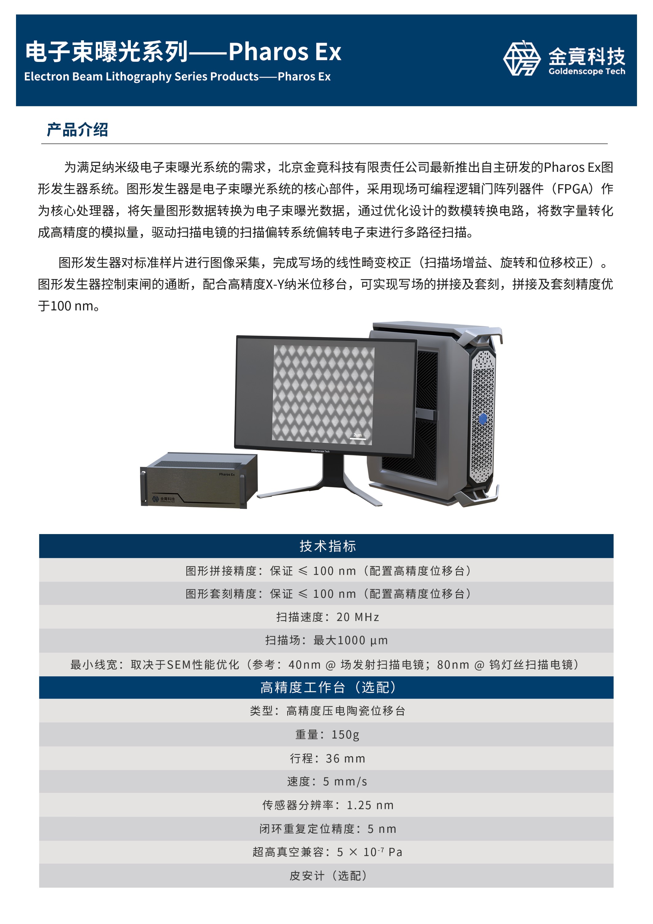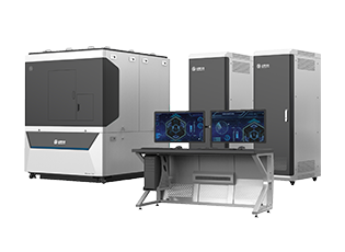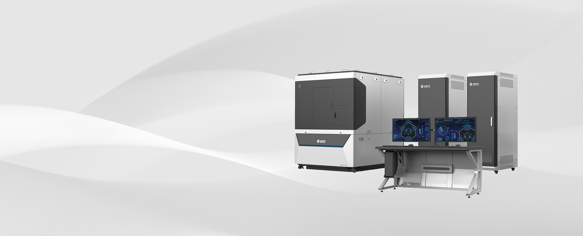


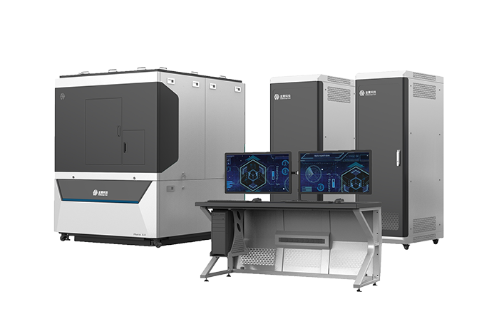
Electron Beam Lithography system——Pharos 510

Electron beam lithography is a high-resolution patterning technology that utilizes a focused high-energy electron beam to directly expose the surface of a wafer, generating micro- and nano-scale structures. The key to this technology lies in its system performance, which determines the critical dimensional accuracy of the final product, the accuracy of pattern stitching, and the consistency of multi-layer overlay.
The Pharos 510 electron beam lithography system, independently developed by Goldenscope Technology, boasts advantages such as high resolution, precise control, and high automation. It is widely used in the fabrication of semiconductor chips, photonic components, and other micro- and nano-structures. It serves as an ideal tool for research and development of submicron to nanometer-scale lithography technology under laboratory conditions.
Applications of Electron Beam Lithography system:
· Semiconductor Manufacturing: Used for the fabrication of integrated circuits, chips, and other semiconductor devices.
· Nanotechnology Research: Plays a crucial role in the development of nanomaterials and nanodevices.
· Optics: Used in the production of photonic crystals, optical waveguides, modulators, metasurfaces, and other optical components.
· MEMS (Micro-Electro-Mechanical System): Utilized in the fabrication of nanostructures.
· Biochips: Applied in the manufacturing of biochips.
· Materials Science: Research on the surface properties and structures of materials.
· Quantum Technology: Used in research and development in quantum computing, quantum communication, and related fields.
Technical Specifications
· Electron emission source : Schottky thermionic field emission source
· Maximum accelerating voltage : 50kV
· Minimum Line Width : ≤10 nm
· Process line width : ≤100nm (Operating conditions: 1nA & 1000μm field)
· Overlay Accuracy : ≤±25nm
· Stitching Accuracy : ≤±25nm
· Maximum Writing Field Size : 1000μm×1000μm(accelerating voltage:50kV)
· Sample size : 2-8 inch wafers and small-sized samples
· Electron beam scanning frequency : ≥100MHz
· Electron beam current : 30pA-100nA
· Positioning method : High-precision vacuum workpiece table positioned by laser interferometer
· Sample stage movement range : 200mm
Performance Configuration
· Eight-level electrostatic deflection
· Automatic focus astigmatism and height measurement
· Automatic sample feeding
· Proximity effect correction
· Cyclic correction function for beam and spot position


Professional Systematic Training


Rich Application Experience


Timely And Efficient Response


Excellent Service Experience


GOLDENSCOPE TECH GOLDENSCOPE TECH GOLDENSCOPE TECH GOLDENSCOPE TECH GOLDENSCOPE TECH GOLDENSCOPE TECH GOLDENSCOPE TECH GOLDENSCOPE TECH GOLDENSCOPE TECH GOLDENSCOPE TECH


 Product Introduction
 Technical Specifications
 Download Center
 Service Support