
APPLICATION

Detection and processing of luminescence signals excited by electron beams are typically combined with scanning or transmission electron microscopy, enabling morphology observation, structure and composition analysis together with electron beam-excited luminescence spectroscopy study. The electron beam used for electron beam-excited luminescence has a very small spot size and high energy. Compared to photoluminescence, electron beam-excited luminescence signals have the advantages of high spatial resolution, strong excitation energy, a wide spectral range, and deep excitation depth. It also enables panchromatic or monochromatic cathodoluminescence Imaging and luminescence surface distribution imaging.
1、The Rainbow series cathodoluminescence imaging and spectral acquisition system enables cathodoluminescence imaging and spectral collection of semiconductor samples, allowing for the detection of emission peaks related to band-edge excitation, defects, quantum wells, and other features in the sample.
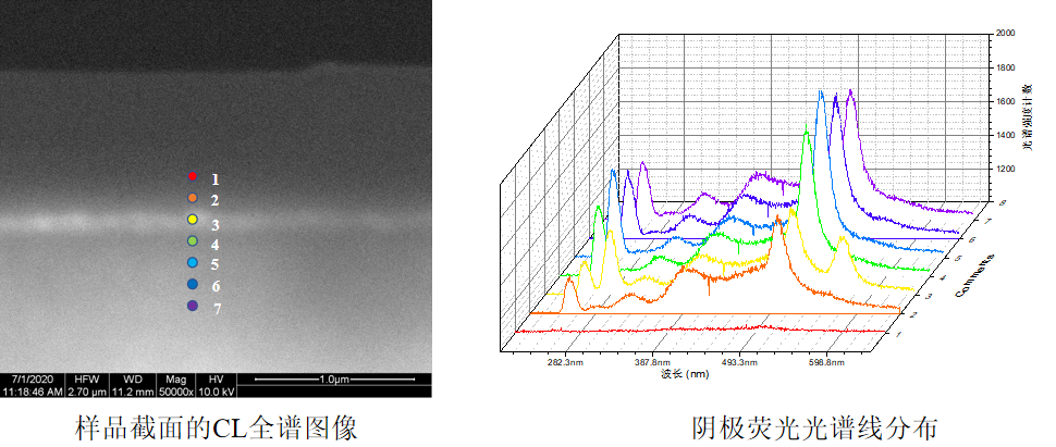
2、DUV LED (sample prepared by FIB) cathodoluminescence imaging and spectral acquisition at specific locations, combined with hyperspectral line scanning, enables high-resolution analysis of semiconductor sample cross-section, allowing observation of luminescence characteristics in different regions.
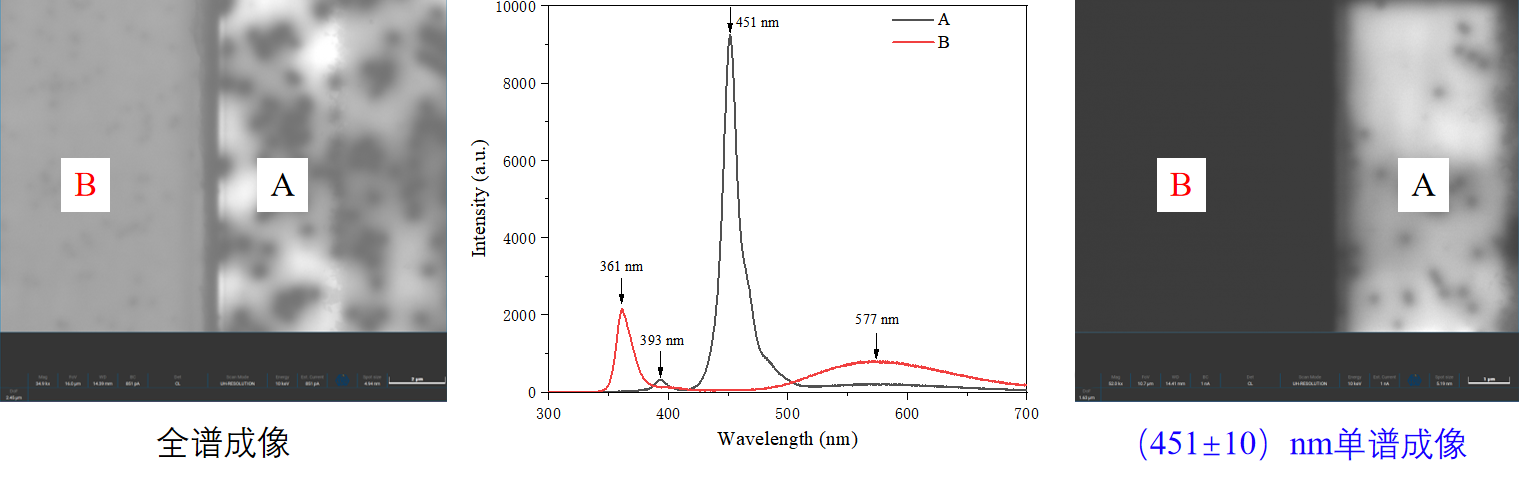
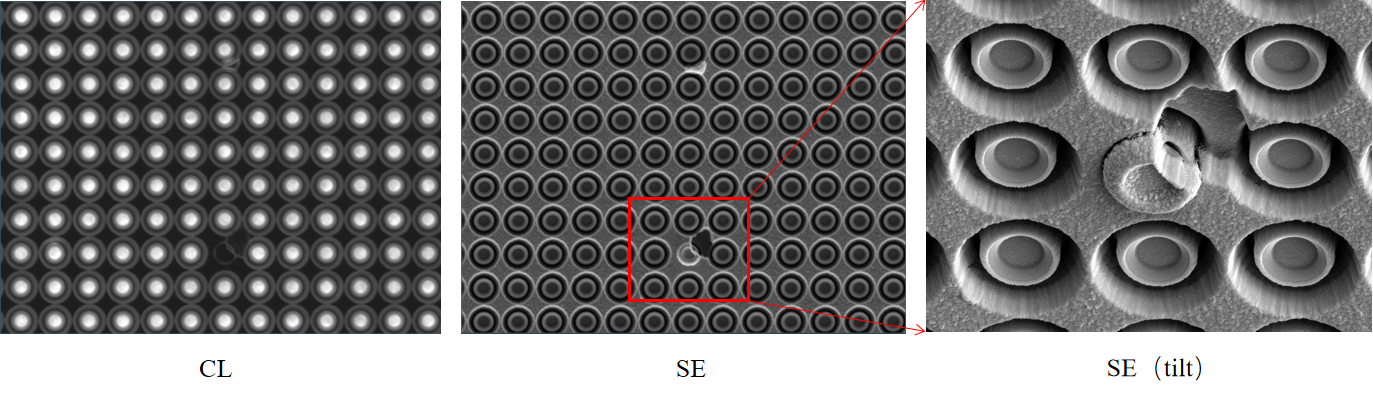
3、Panchromatic + Monochromatic Imaging of Mini LED Samples,The Rainbow series enable monochromatic CL imaging on specific spectral band of interest.
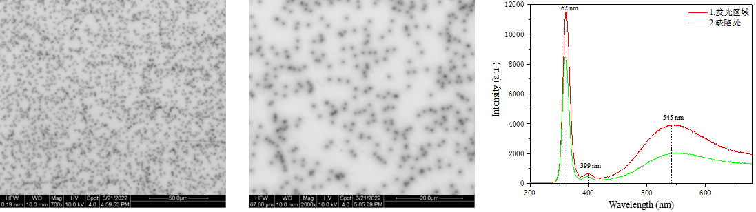
4、The Rainbow series enable cathodoluminescence imaging and spectral acquisition of different characteristic regions on Micro LED epitaxial wafers.

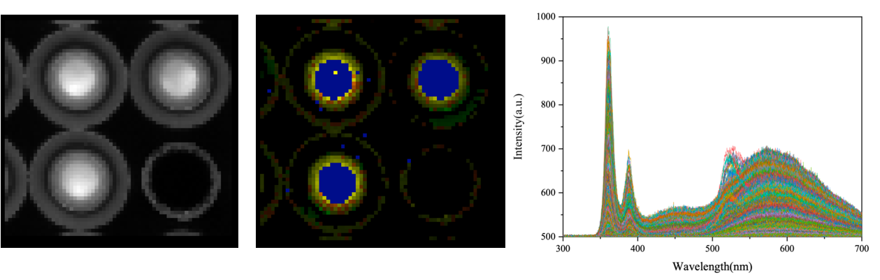
5、Spectral surface analysis allows simultaneous observation of CL image and spectral information in micro-areas of Micro LED, presenting the true luminescent color distribution of the sample.
6、For LED samples, the Rainbow series provides luminescence intensity distribution maps of different regions.
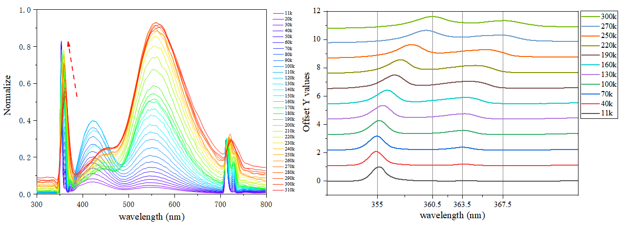
7、The Rainbow system, combined with our cryostage, enables observing the effect of different temperatures on GaN spectra.
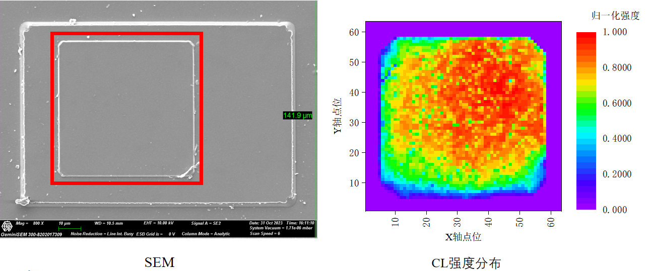
8、Failure Analysis of Semiconductor Devices. Defect Analysis of Micro LED Samples ( Part of gold layer on the surface was not etched away, affecting the light output of the LED device).


GOLDENSCOPE TECH GOLDENSCOPE TECH GOLDENSCOPE TECH GOLDENSCOPE TECH GOLDENSCOPE TECH GOLDENSCOPE TECH GOLDENSCOPE TECH GOLDENSCOPE TECH GOLDENSCOPE TECH GOLDENSCOPE TECH